




4 Semiconductor Machine Parts to Redesign using 3D Printing
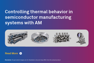
Every chip inside your phone, laptop or car is made on highly precise machines, known as semiconductor manufacturing equipment. These machines handle gases, liquids, heat and silicon wafers with extreme accuracy, often inside a vacuum and a cleanroom. The chips themselves are not 3D printed. However, many of the metal parts inside these machines can be, and in some cases they perform better than parts made the conventional way.
This is a large and growing market. Worldwide billings for semiconductor manufacturing equipment reached $135.1 billion in 2025, 15% higher than in 2024 [1]. Most of this equipment, including the wafer fab equipment used for lithography, deposition and etching, is assembled by a small group of global OEMs, who buy many of the parts from specialist suppliers. For these suppliers, additive manufacturing (AM), also known as metal 3D printing, is worth a closer look wherever drilling, brazing, welding or joining many small pieces limits how well a part can perform.
That said, the aim is not to 3D print every part. The aim is to pick the right parts, redesign them around the job they actually do, and then prove the improvement with real test data on flow, temperature, strength, cleanliness and cost.
Which parts of semiconductor manufacturing equipment suit additive manufacturing?
In metal additive manufacturing, a laser melts fine metal powder layer by layer to build a part. This process is called laser powder bed fusion (LPBF). Since the part is built up layer by layer, it can have hollow channels, very thin walls and complex internal shapes that no drill or cutting tool can reach. In semiconductor equipment, this matters most for four types of parts.
Gas and fluid manifolds
A manifold is a metal block that routes process gases or liquids to different sections of the machine. Conventionally, it is made by drilling straight holes into a solid block, plugging the extra openings and then brazing or welding several pieces together. The drilled paths create sharp turns and dead corners where the flow slows down or gets trapped, and every joint is a possible leak point.
With AM, the internal passages can follow a smooth, curved path, and many separate pieces can be combined into a single part. In one published semiconductor example, more than 20 parts were combined into one manifold. The supplier reported a 90% drop in flow-induced disturbance forces and linked it to a 1 to 2 nm improvement in accuracy [2]. For the equipment maker, this also means fewer parts to buy, inspect and assemble, and a more compact unit.
Before such a manifold goes into a tool, it has to be checked for corrosion resistance, outgassing, helium leak tightness, cleanliness and particle levels, and proper passivation of the metal surface.
Wafer tables and wafer chucks
The wafer table, or wafer chuck, holds the silicon wafer in place while it is exposed, measured or inspected. Even a small temperature difference across its surface can affect accuracy. The machine also often has to wait for the table to settle at a stable temperature before it can continue, which costs production time.
AM allows cooling channels to closely follow the shape of the table, known as conformal cooling, and to use internal lattice structures with a large surface area. This brings the cooling much closer to the surface that needs to stay stable. Published concepts report temperature gradients below 4 mK, which is four thousandths of a degree, and thermal time constants below 1.5 seconds, meaning the table responds quickly to temperature changes [3]. In a study on a 12-inch wafer chuck, an optimised lattice design (diamond TPMS) kept the surface temperature difference to 0.23 °C, compared with 0.66 °C for another lattice design (gyroid) [4].
For these parts, testing focuses on thermal conductivity, thermal expansion, flatness, temperature uniformity and coating adhesion. Any gain in settling time or tool productivity also needs to be confirmed on the full machine.
Linear-stage cooling jackets
A linear stage is the platform that moves the wafer or an optical component quickly and precisely. The motors, bearings and position sensors on it produce heat right next to the most sensitive structures. The usual solution is a cooling jacket, often made from welded pieces and connected with fittings, which adds more parts and more leak points.
With AM, the cooling jacket can be built as one part, with the channels placed exactly where the heat is produced and no welds or fittings needed. One published application reports combining eight parts into one, walls just 0.6 mm thick and 75% less time to produce the component [5]. In practical terms, this means fewer suppliers, a shorter assembly process and fewer places where coolant can leak.
These parts are tested for fatigue, stiffness, coolant compatibility, pressure and leak performance, and response to temperature changes. CT scanning is often used to confirm that the internal channels are clear and correctly formed.
Flexures, optical mounts and precision brackets
A flexure is a part that allows very small, controlled movement by bending, instead of using hinges or bearings. Along with optical mounts and precision brackets, these parts need to be stiff enough to hold their position but light enough to move quickly. When they are built from several pieces, small errors add up at each joint, and technicians spend time adjusting them during assembly.
AM, combined with a design method called topology optimisation, removes material from areas that carry no load while keeping the part stiff where it matters. Mounting points can also be built into the part itself. Lower weight allows faster acceleration, and fewer joints mean smaller accumulated errors and less adjustment time [3].
For these parts, the key checks are fatigue life, vibration behaviour, dimensional stability and how accurately the part returns to the same position every time [3].
Which materials are used for these parts?
The choice of material depends on what the part will face inside the machine: the chemicals, vacuum, temperature, loads, surface finish and cleanliness requirements [2][5]. Among metals, 316L stainless steel is a common choice for corrosion-resistant manifolds and vacuum hardware. AlSi10Mg, an aluminium alloy, is widely used for lightweight thermal parts. Titanium suits structures that need to be stiff yet light, and nickel alloys are used in hotter or more chemically aggressive conditions.
Aheadd® CP1 for heat-management parts
Aheadd® CP1 is an aluminium alloy, made with iron and zirconium, that was developed specifically for laser powder bed fusion. According to its data sheet, it offers high thermal and electrical conductivity, strength and ductility similar to 6000-series aluminium alloys, and good corrosion resistance. It can be anodised and polished, and it stays stable at temperatures up to 300 °C [6]. Its listed uses include manifolds, heat exchangers, cooling systems, mixers and flow optimisers [7].
This makes CP1 a good candidate for wafer tables, cooling jackets and compact 3D printed heat exchangers. It also needs only a single heat-treatment step with no quenching, which can make post-processing simpler [6]. Like any material, it still needs to be tested for outgassing, cleanliness, coatings and compatibility with each tool's process.
Ceramics where metals reach their limits
Some parts need properties that metals cannot offer, such as electrical insulation or very high chemical resistance. This is where ceramics come in. Alumina offers electrical insulation, chemical resistance and high purity. Aluminium nitride conducts heat well while still insulating electrically. Silicon carbide is stiff, wear-resistant and holds its shape, while silicon nitride is strong and handles sudden temperature changes well.
Ceramic AM can produce wafer-handling blades, chuck features, insulating fixtures, nozzles and guides, including parts with internal channels for gas, suction or cooling. For example, Bosch Advanced Ceramics reports a single-piece ring blade for handling 200 mm wafers, made from alumina of more than 99.8% purity. It has a 120 mm internal channel, weighs 280 g and is flat to within 100 µm [8]. Ceramic parts do need careful control of shrinkage, sintering, density and surface finish, since ceramics can crack more easily than metals [9].
How do these engineering gains turn into business value?
In semiconductor capital equipment, a printed part is worth it only if the benefit shows up on the machine or in the supply chain. The table below connects each design advantage to the business case a customer would build around it.
Design advantage | What changes on the machine | How to build the business case |
Part consolidation | Fewer joints, seals, drawings, suppliers and inspections | If a brazed manifold becomes one qualified part, compare the saved assembly, leak-testing, rework and inventory cost against the full AM route. |
Conformal flow or cooling | Less disturbance, faster temperature settling and more compact design | If settling time limits machine availability, calculate the machine hours gained each year from the measured time saving. |
Lighter parts with the same stiffness | Lower moving weight and potentially faster motion | Compare the throughput gain from tested speed improvements against the redesign and qualification cost. |
Digital, tool-less production | Faster design changes and affordable low-volume variants | Compare conventional tooling and long-lead inventory with the lead time for qualified repeat builds. |
High-performance materials | Thermal, electrical, chemical or vacuum properties matched to the part | Assess CP1 or ceramics where better performance can reduce cooling needs, contamination risk, service visits or part count. |
What this means for your team
For design and mechanical engineers: AM removes many limits that engineers usually design around, such as drill paths, braze joints, fittings and weld access. A good question to ask is: which part in our current assembly is held back by the way it has to be made? That part is the right one to evaluate first.
For product and business leaders: The business case rests on outcomes you can measure, such as fewer parts and suppliers, shorter assembly time, fewer leak points, faster temperature settling and less dependence on long-lead supply. AM can make financial sense even at modest volumes, where complexity, qualification, machine uptime or supply continuity matter more than the price of a single part.
How to get started
The best way to begin is with one part. Choose a component that has a known problem, such as a leak-prone joint, uneven cooling or a long lead time, and for which you already have baseline numbers on flow, temperature, part count, lead time or cost.
Next, compare design options through simulation, such as flow (CFD), thermal or structural analysis, before anything is printed. Once a design looks promising, build a sample part and test its material properties, dimensions, internal channels, leak tightness, cleanliness and actual performance. CT scanning helps inspect internal features that cannot be seen otherwise.
When comparing costs, look at the total cost and not just the price per part. The conventional route includes sub-parts, joining, seals, cleaning, inspection, scrap, inventory, urgent delivery charges and field-service issues. Move to qualification and regular production only when the tested benefit clearly outweighs the development and qualification effort.
How Wipro 3D supports semiconductor equipment makers and suppliers
Wipro 3D is a metal additive manufacturing company based in Bengaluru, India, and already supplies additively manufactured parts to the semiconductor equipment industry. We understand what this sector expects: precision, reliable internal channels, cleanliness, full traceability, controlled post-processing and consistent quality.
We work with customers at every stage, from identifying the right application to design for AM, material and process selection, simulation, prototyping, post-processing, inspection, qualification and repeat production. This helps answer two questions together: can this part be printed, and will the complete manufacturing and validation route deliver measurable value?
Most engagements begin with a non-confidential component review, followed by a step-by-step feasibility study and a qualification plan based on test evidence.
References
[1] SEMI, “Global Semiconductor Equipment Billings Reached $135.1 Billion in 2025,” 2026.
[2] 3D Systems, “Manifold Fluid Flow Optimization.”
[3] 3D Systems, “Additive Manufacturing for Semiconductor Capital Equipment.”
[5] 3D Systems, “Linear Stage Cooling.”
[6] Nikon SLM Solutions, “Aheadd® CP1 Material Data Sheet.”
[7] 3D Systems, “Aheadd® CP1 Aluminum Alloy.”
[8] Ceramic Applications, “Leveraging Ceramic AM for Automated Semiconductor Handling.”
Frequently Asked Questions
Next step
Do you have a manifold, thermal body, cooling jacket or bracket that is limited by the way it is made? Share a non-confidential drawing with our applications team for a component review.